
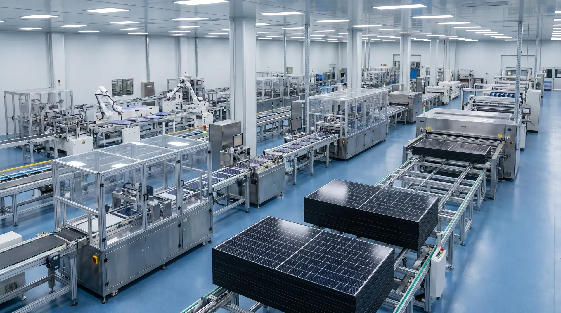


Making a solar panel means following a single, unforgiving chain from quartz sand to a sealed, tested module ready for a roof.
What makes this worth understanding is how tightly each stage depends on the one before it.
Purity sets the ceiling for crystal growth, crystal quality sets the ceiling for the wafer, wafer quality determines how well the cell converts light, and nothing is recoverable downstream.
Walk that chain with me, and the number on any spec sheet will start making a lot more sense.
Why Silicon? What Makes It Turn Sunlight into Electricity
Silicon sits between conductor and insulator on the conductivity scale. Copper conducts freely. Rubber blocks completely. Silicon does neither, and that middle ground is exactly what makes it useful as a solar cell material.
How a Photon Becomes Current
When a photon strikes a silicon atom, it knocks an electron loose. A free electron on its own doesn’t produce electricity, though. You need electrons moving in a direction, and that needs a clean path through the material.
Why Impurities Are a Real Problem
Here’s where impurity atoms do real damage. An impurity atom has a different electron structure than silicon. That difference creates a small trap inside the lattice. A freed electron falls into it instead of traveling toward the metal contacts. That energy becomes heat, not current.
I’ve seen people treat purity requirements as a formality. Trust me they’re not. Each impurity atom is a real drain on output; measurable, consistent, and cumulative across millions of atoms in a single wafer.
The 99.999% Threshold
The line that matters commercially is around 99.999% pure.
Below it, traps are common enough to show up in efficiency readings. Above it, returns shrink; you’re optimizing past the point where impurities are the main problem.
Crystal structure takes over from there.
Even high-purity silicon can grow traps during crystal growth if the temperature isn’t controlled tightly. Purity at input doesn’t guarantee purity in the finished ingot.
Refining sets the ceiling, and the crystal process determines whether you reach it.
From Sand to Silicon Ingot: Purification and Crystal Growth
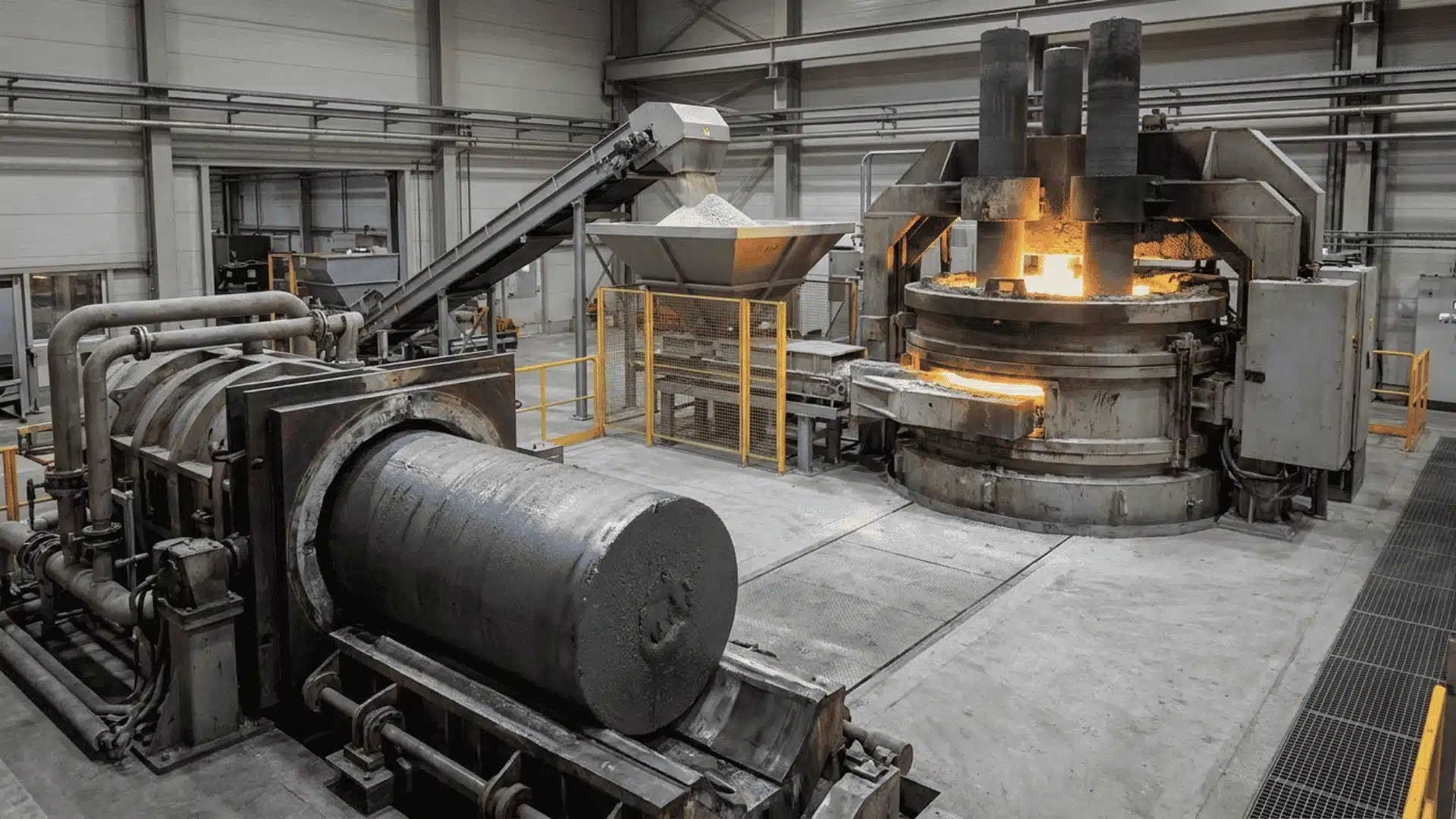
Every solar panel starts as quartz sand, which is silicon dioxide pulled from the ground.
Two things have to happen before any cell work begins: chemical purification to reach the purity level the process needs, and crystal growth to shape that silicon into a solid block the rest of the line can cut from.
Metallurgical-Grade to Polysilicon
Quartz sand goes into an arc furnace at very high heat. The oxygen burns off, leaving metallurgical-grade silicon at around 99% purity. That sounds high, but in reality it isn’t high enough.
A second pass through a chemical purification cycle, most commonly the Siemens process, where silicon reacts with hydrogen chloride and then breaks down again at high temperature, strips out the rest of the impurities.
Purity reaches 99.999% or higher. The result is polysilicon: the starting material for every ingot on the line.
Monocrystalline vs. Polycrystalline Ingots
With polysilicon ready, you melt it and grow it into ingots. The method you pick here shapes the kind of cell you end up with, and that choice is about cost as much as performance.
The Czochralski process dips a seed crystal into the melt and pulls it upward slowly. A single continuous lattice grows with no grain boundaries. That’s a monocrystalline ingot. Cast ingots cool in a mould instead, solidifying in multiple directions and building a patchwork of crystal grains. That’s the polycrystalline route.
Grain boundaries scatter electrons slightly and pull efficiency down. But casting is simpler and cheaper. For utility-scale projects where cost-per-watt is everything, the trade-off makes sense. For a residential roof where space is the constraint, monocrystalline usually wins.
Why Ingot Quality Determines Everything Downstream
A defect born at the ingot stage travels with the silicon. Oxygen contamination during Czochralski growth creates lattice defects that carry into the wafer. Uneven cooling in casting produces stress points that crack during slicing.
In my experience, this is the most underestimated stage in the whole process.
Nearly all measurable yield loss in solar manufacturing traces back here, and almost none of it can be fixed once the ingot has solidified. By the time a defect shows up in the final flash test, it was born right here.
Getting the crystal right isn’t one step among many. It’s the foundation every other step stands on.
From Silicon Wafer to Solar Cell: Doping, the PN Junction, and Contacts
This is where refined silicon stops being a material and becomes a device. By the end of this stage, you have something that actually generates electricity when light hits it.
The wafer gives you the base, doping gives it electrical properties, and the p-n junction is where the photovoltaic effect lives.
Slicing Wafers and Why Thickness Matters
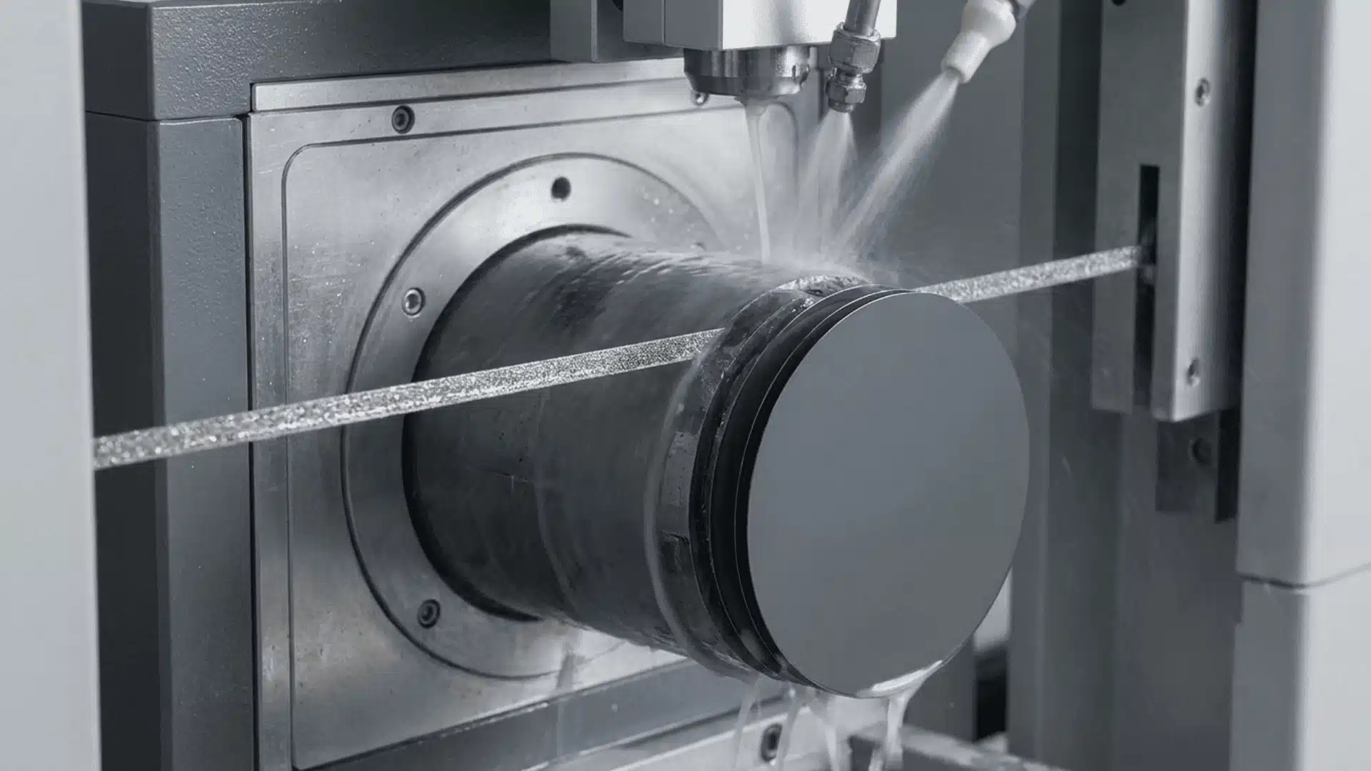
Ingots get sliced into wafers using diamond-wire saws that have wires coated in diamond particles that cut through silicon with minimal force.
Target thickness is 170–200 micrometers, roughly twice the width of a human hair.
Thickness is a cost equation. Thinner wafers use less silicon per cell. Go too thin, and the wafer becomes fragile, prone to cracking in handling.
The material lost to the cut is called kerf loss. Less kerf means more cells from the same ingot, which is why diamond-wire replaced slurry-wire saws. It cuts a narrower path and gets more usable material from each kilogram of polysilicon.
Doping: Building the P-Type and N-Type Layers
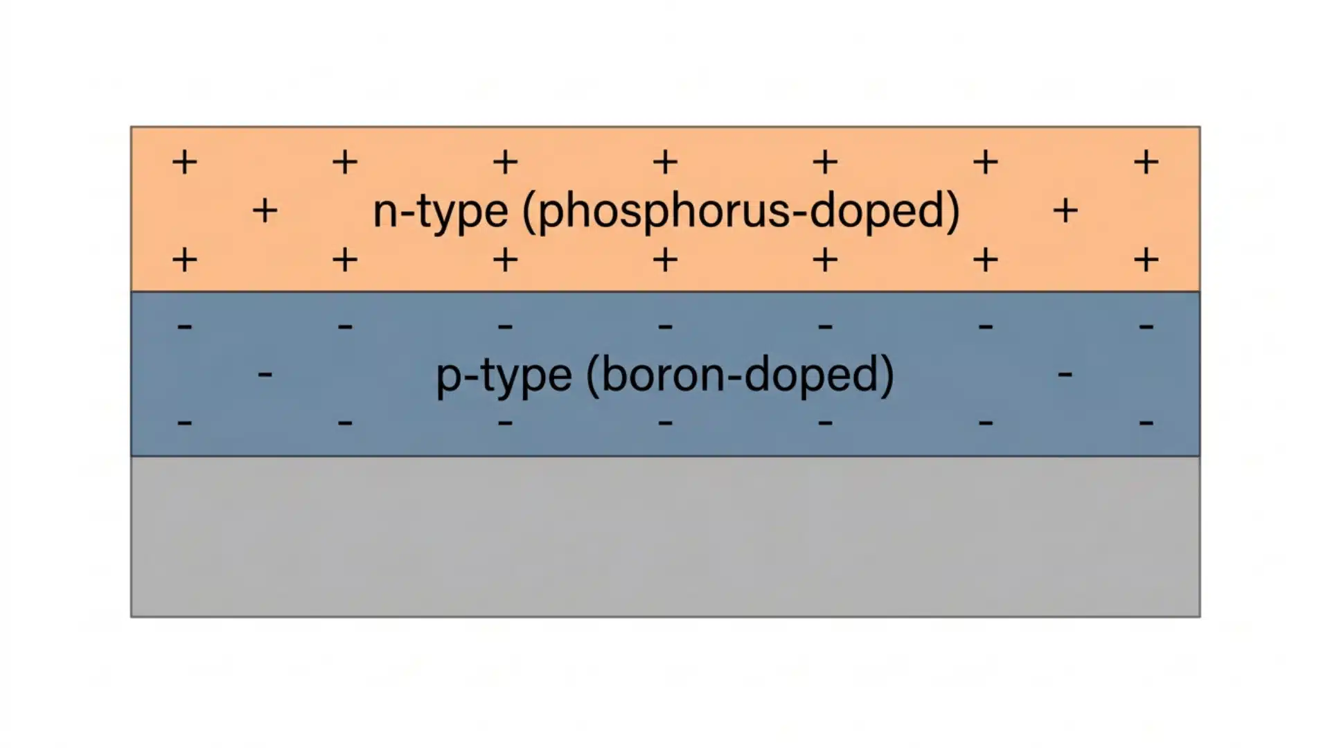
A pure silicon wafer doesn’t generate electricity on its own. Doping fixes that by pushing foreign atoms into the silicon in controlled amounts, small enough not to break the lattice, large enough to shift its electrical character.
Borongoes into the bulk of the wafer. Boron has one fewer electron than silicon, so it creates a region that pulls electrons toward it, the p-type layer.
Phosphorusgoes in at the surface. It has one extra electron, creating a region of surplus charge, the n-type layer.
These two layers sitting against each other set up everything that comes next.
The P-N Junction and Why It Generates Current
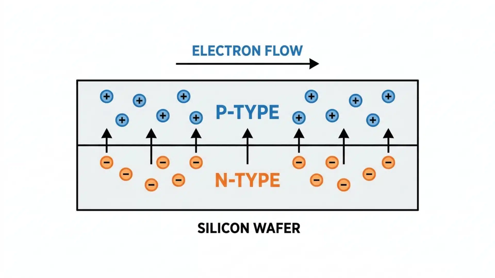
Where the p-type and n-type layers meet, electrons from the n-side drift across and fill holes on the p-side. That movement creates a built-in electric field pointing from n to p. The field is the engine of the whole device.
When a photon knocks an electron loose, the field pushes it toward the n-side. The hole left behind gets pushed toward the p-side. That split is what drives current through the circuit.
Without the field, freed electrons wander and recombine. The p-n junction gives them a direction. If you want to understand why solar cells work at all, this is the answer: not the silicon itself, but the interface between two differently doped regions of it.
Anti-Reflective Coating and Metal Contacts
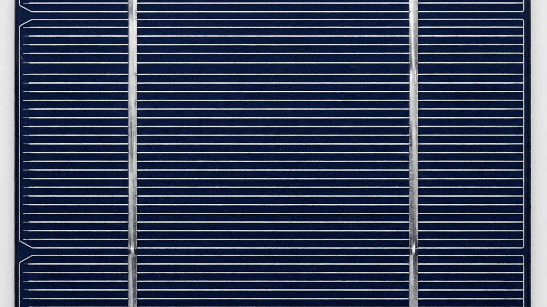
Bare silicon reflects about 35% of incoming light. That’s 35% of available energy that never enters the cell.
An anti-reflective coating drops that to around 3%. You’re not changing the cell’s physics here, you’re letting more light reach the junction that was always there.
Metal contacts then get screen-printed onto the cell in a grid: silver pasteon the front, aluminum pasteon the rear. These collect the current that the p-n junction produces and carry it out of the cell.
The front grid is a real trade-off, and it’s one I think gets underappreciated. Wider fingers collect current better but block more light. Narrower fingers let more light through but they add resistance.
That balance is where a big chunk of the efficiency number on a spec sheet gets decided, and it’s why two panels at the same nominal rating can perform differently once they’re on a roof.
Assembling the Module: Stringing, Lamination, Framing, and Protection
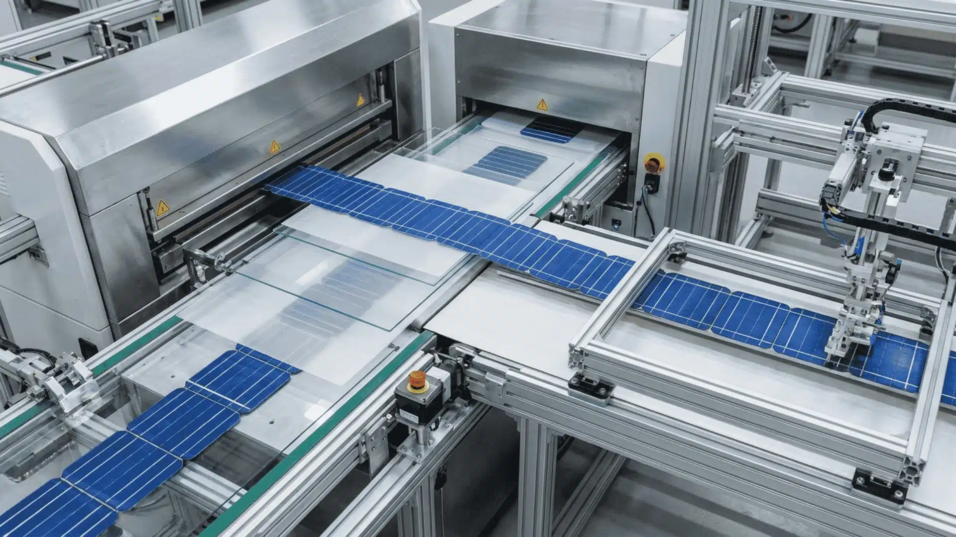
A single solar cell is fragile, exposed, and electrically cut off from everything. Module assembly turns a grid of individual cells into a sealed, weatherproof unit that can bolt to a roof and connect to a system. Every layer and component here has a specific job.
Stringing Cells into a Matrix
Individual cells get connected with thin copper ribbons soldered across their front and back contacts.
Automated stringer machines do this at speed with consistent pressure, more consistent than any human hand at scale.
Cells are wired in series to raise voltage. Those strings run in parallel to raise current. Together, that configuration sets the panel’s electrical output.
A misaligned ribbon or a cold solder joint creates a weak spot that often stays hidden for months in the field, which is why stringer calibration matters just as much as the cell quality going into it.
What Each Layer of the Laminated Stack Does
The laminated structure has five layers. Each one has a job, and swapping in cheaper materials anywhere in the stack isn’t a minor cost decision; it’s a choice that plays out in how long the panel lasts.
Tempered glassgoes on top: low-iron to cut light absorption, and tempered to handle mechanical load.
Below that comes the first layer of EVA (ethylene vinyl acetate), a clear polymer. Then the cells. Then a second EVA layer. Then a polymer backsheet as the rear moisture barrier and electrical insulator.
EVA is the bond that holds everything together, and I think it’s the most overlooked part of the whole structure. During lamination, the panel goes into a vacuum press under heat.
The EVA cross-links into a polymer network; it doesn’t just stick, it chemically bonds to the glass, the cells, and the backsheet. That’s what makes the interior moisture-proof.
The frame seals the edges, sure, but the EVA seals everything inside.
Framing, Junction Box, and Bypass Diodes
An aluminum frame seals around the panel, giving it structural rigidity and the mounting points needed for installation. The frame also protects the glass edges; a chip there spreads inward under thermal cycling in a way a central impact usually doesn’t.
A weatherproof junction box on the rear is where the panel’s electrical output leaves through cables and connectors.
Inside sit bypass diodes. When a cell gets shaded, it resists current and forces nearby cells to burn off that energy as heat. Bypass diodes short-circuit shaded cells before that hotspot builds.
A failed bypass diode doesn’t kill the panel right away. It lets hotspot damage build quietly, which is exactly why bypass diode health is part of any serious field inspection. The harm compounds long before it becomes visible.
How a Panel Gets Its Wattage Rating: Flash Testing, Infrared Scanning, and Binning
A solar panel’s wattage rating is a measured result, not a design goal. Every panel gets tested individually before it ships, and the number on the label is what that specific panel actually produced under controlled conditions.
The Flash Test
Each panel takes a calibrated pulse of simulated sunlight at the AM1.5 spectrum; the standard for sunlight filtered through the atmosphere at a typical angle, at 1,000 W/m² and 25°C cell temperature.
The electrical output recorded in that instant is the rated wattage. This is not a class average; it’s the real output of that panel.
Why Binning Exists
Panels that test below their target go through binning.
A panel built to a 400W spec that flashes at 392W doesn’t get scrapped. It gets relabeled as 392W and sold at that rating. The buyer gets an honest number. The manufacturer gets revenue from a working module instead of a write-off.
This is also why two panels with the same model number can carry slightly different output figures.
Infrared Scanning
Infrared scanning runs alongside flash testing. Thermal imaging finds EVA delamination and micro-cracked cells that look fine to the eye.
I think of IR scanning as the check that catches the quiet problems, the ones that won’t surface for years in the field but will eventually trigger a warranty claim.
Most legitimate warranty disputes involve defects that infrared scanning at the factory would have caught.
What Every Step Adds Up To
Knowing how solar panels are made changes how you read a spec sheet. The efficiency number reflects decisions made at crystal growth, doping, contact grid design, and the flash test; not one choice, but every stage compounding on the one before it.
A panel that still performs well after ten years got there because the ingot was clean, the EVA cross-linked properly, the bypass diodes held, and the infrared scan caught what the visual inspection missed.
Quality here is cumulative. Each stage either builds on a solid base or tries to work around a weak one. The ones it can’t work around show up eventually.
Frequently Asked Questions
What is the difference between monocrystalline and polycrystalline solar panels?
Monocrystalline panels come from a single continuous silicon crystal grown using the Czochralski process, giving electrons a clean, uninterrupted path through the material. Polycrystalline panels are cast from molten silicon that solidifies in multiple directions, forming grain boundaries that scatter electrons slightly. Monocrystalline panels typically reach 20–23% efficiency; polycrystalline panels sit closer to 15–18%. The gap narrows as manufacturing improves.
Why does silicon purity matter for solar panel performance?
Impurity atoms in the silicon lattice have a different electron structure than silicon, creating small energy traps that freed electrons fall into instead of flowing toward the contacts. That energy turns into heat. At 99.999% purity, these traps are rare enough that the cell converts most incoming light into current. Below that threshold, the efficiency loss is measurable and consistent.
What does the EVA layer in a solar panel actually do?
EVA wraps around the silicon cells and bonds the glass, cells, and backsheet into one sealed unit during vacuum-heat lamination. Under heat and pressure, EVA cross-links into a polymer network, making the bond permanent and keeping moisture out. Without it, the cells stay loose and exposed. Most panel delamination failures in the field trace back to EVA breaking down over time.
How is a solar panel’s wattage rating determined?
Wattage gets measured during a flash test, a calibrated pulse of simulated sunlight at AM1.5 spectrum, 1,000 W/m², and 25°C cell temperature. The electrical output in that instant becomes the rated wattage. Panels that test below their target class get binned into a lower rating and sold at that label, not thrown away.